找回密码
 免费注册

QQ登录

只需一步,快速开始

北京中仪天信科技有限公司 江苏东方航天校准检测有限公司 热处理论坛合作伙伴广告位
搜索
楼主: leomet

[求助] 馬氏体不銹鋼 金相照片

[复制链接]

签到天数: 474 天

[LV.9]以坛为家II

 楼主| 发表于 2015-10-21 11:22:01 | 显示全部楼层
北京中仪天信科技有限公司
本帖最后由 leomet 于 2016-6-13 07:27 编辑
shenfuhai 发表于 2014-9-22 10:01
谢谢吴老师指导。

420不锈钢,我曾经加热到1100度,碳化物完全固溶;然后淬火,晶粒大的出奇。


好像只有你認同我的"双晶"說.........

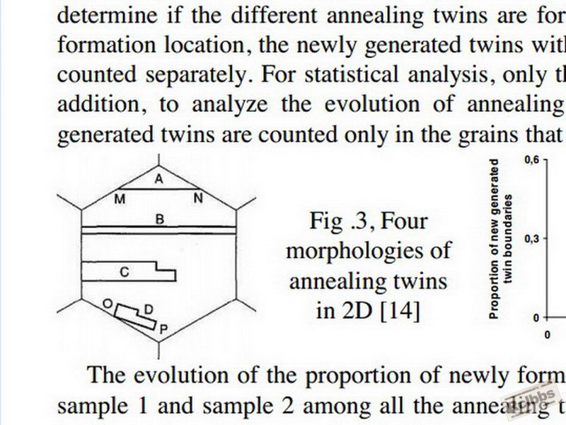
我的照片中 有的Twin 形貌 還不包括在這四個形貌呢.
twin shapes 1.jpg
回复

使用道具 举报

签到天数: 474 天

[LV.9]以坛为家II

 楼主| 发表于 2016-8-21 15:25:02 | 显示全部楼层
本帖最后由 leomet 于 2016-8-21 16:09 编辑


Twin boundary Carbide. Scroll up the 2nd photo to see the thickness of the twin carbide.

TAZ company , Germany
k.jpg
TAZ Twin Karbid.jpg
回复

使用道具 举报

签到天数: 474 天

[LV.9]以坛为家II

 楼主| 发表于 2016-8-21 15:28:25 | 显示全部楼层
X46Cr13  Martensitic stainless steel
bad carbide.jpg
Carbide.jpg
Karbid.jpg
stainless steel.jpg
x 420 J2.jpg
X46Cr13.jpg
回复

使用道具 举报

签到天数: 474 天

[LV.9]以坛为家II

 楼主| 发表于 2016-8-21 15:33:42 | 显示全部楼层
本帖最后由 leomet 于 2016-8-21 16:53 编辑

偏析非常嚴重...................擴散退火未做(好)?
最下面照片中 白色網線是 鍛塊遺留下來的晶界.
三個黑"點"是嚴重偏析處.
Good carbide: well-dispersed carbide particles.
Bad carbide: continuous carbide particles.
IMAG0212.jpg
IMAG0230.jpg
IMAG0231.jpg
zd.jpg
00 IMG_8980.jpg
0 IMG_8957.jpg
0 IMG_8979.jpg
回复

使用道具 举报

签到天数: 474 天

[LV.9]以坛为家II

 楼主| 发表于 2016-8-21 15:42:47 | 显示全部楼层
本帖最后由 leomet 于 2016-8-26 10:08 编辑

SEM photos of this steel......................
Very flat fracture grain surfaces are twins.
0 37.jpg
0 81 吳.jpg
0 84.jpg
0 85.jpg
回复

使用道具 举报

签到天数: 474 天

[LV.9]以坛为家II

 楼主| 发表于 2016-8-21 15:51:36 | 显示全部楼层
本帖最后由 leomet 于 2016-8-21 17:40 编辑

This pellet-making tooling fractured in one day, and one day only !
Tooling was sent back from North America.
Grains flaked off the surface like this in one day.
Toughness of the Q/T steel must be very, very BAD !
5 b.jpg
5 b1.jpg
5 c.jpg
5 c1.jpg
5 c2.jpg
5 c3.jpg
5 c5.jpg
回复

使用道具 举报

签到天数: 474 天

[LV.9]以坛为家II

 楼主| 发表于 2016-8-21 15:57:47 | 显示全部楼层
本帖最后由 leomet 于 2016-8-21 15:59 编辑

Fracture surface taken with USB microscope.
Note those very flat and reflective twin surfaces.
1 a.jpg
1 aa.jpg
1za.jpg
3 b.jpg
1608021802501450419.jpg
ZQ6.jpg
回复

使用道具 举报

签到天数: 474 天

[LV.9]以坛为家II

 楼主| 发表于 2016-8-21 16:07:15 | 显示全部楼层
Do you get the whole picture?  You young and promising engineers.
0 .jpg
0 1 a.jpg
回复

使用道具 举报

签到天数: 474 天

[LV.9]以坛为家II

 楼主| 发表于 2016-8-21 16:19:00 | 显示全部楼层
本帖最后由 leomet 于 2016-8-24 18:00 编辑

OM Microstructure.....................
Carbide tinted in 2nd and 3rd photo.
01 Twin Carbide.jpg
1 IMG_8159a.jpg
1 IMG_8166.jpg
1IMG_8139.jpg
回复

使用道具 举报

签到天数: 474 天

[LV.9]以坛为家II

 楼主| 发表于 2016-8-21 16:28:34 | 显示全部楼层
本帖最后由 leomet 于 2016-8-21 19:09 编辑

Color etching.........................
See the last photo, 1 aa 4.jpg,  you can see that density of twin carbide is very high, indeed.
0 .jpg
0 1.jpg
0 12.jpg
0 aa 2.jpg
0 IMG_8530a.jpg
0 IMG_8532.jpg
0 IMG_8535.jpg

twin carbides

twin carbides
回复

使用道具 举报

签到天数: 474 天

[LV.9]以坛为家II

 楼主| 发表于 2016-8-21 16:42:42 | 显示全部楼层
I hope you young metallurgists enjoy reading these beautiful and instructive metallographic photos presented by the old man from Central Taiwan.
回复

使用道具 举报

签到天数: 474 天

[LV.9]以坛为家II

 楼主| 发表于 2016-8-21 17:48:19 | 显示全部楼层
本帖最后由 leomet 于 2016-8-21 17:50 编辑

These photos of secondary cracking also show evidence
that twin carbides are the weakest sites of the steel.
No doubt about it.
IMG_8693.jpg
IMG_8694.jpg
IMG_8695.jpg
IMG_8696.jpg
IMG_8697.jpg
IMG_8698.jpg
IMG_8700.jpg
回复

使用道具 举报

签到天数: 608 天

[LV.9]以坛为家II

发表于 2016-8-24 08:16:52 | 显示全部楼层
leomet 发表于 2014-9-22 19:17
那2張影印的照片來自一份台灣權威單位(MIDRC, 金屬中心)的分析報告. 不知哪個經驗太稚嫩的小朋友分析的 ...

吴先生,我今日偶然看到此贴。

本人非常认同吴先生的看法。原两粗晶的金相图片,主要是锻造过程未细化晶粒所致。
回复

使用道具 举报

签到天数: 474 天

[LV.9]以坛为家II

 楼主| 发表于 2016-8-24 18:11:10 | 显示全部楼层
本帖最后由 leomet 于 2016-8-26 10:06 编辑

leomet 发表于 2016-8-21 15:57
Fracture surface taken with USB microscope.
Note those very flat and reflective twin surfaces.


SEM photos of this cracked surface.

You never see fracture surface with so many twin boundary carbide like this.
43.jpg
47.jpg

twin boundary crack surfaces

twin boundary crack surfaces
回复

使用道具 举报

签到天数: 474 天

[LV.9]以坛为家II

 楼主| 发表于 2016-8-24 18:33:05 | 显示全部楼层
本帖最后由 leomet 于 2016-8-26 10:04 编辑
shenfuhai 发表于 2014-9-21 22:11
吴老师好。这个粗大的晶界是原材的遗留的;晶界非常清晰,估计于在1030度保温时间过短有关系,从晶界碳化物 ...


這些平行線是魏先生碳化物, 與双晶碳化物有別.........
不是搞高Cr鑄造的, 難得見到它. 我只看過這一次. 所以用SEM把它記錄起來.
Carbide 魏氏.jpg
回复

使用道具 举报

签到天数: 1288 天

[LV.10]以坛为家III

发表于 2018-4-1 21:45:38 | 显示全部楼层
大佬聊天,新手学习!
回复

使用道具 举报

您需要登录后才可以回帖 登录 | 免费注册

本版积分规则

QQ|Archiver|手机版|小黑屋|热处理论坛 ( 苏ICP备2021037530号|苏公网安备32059002001695号 )
Copyright © 2005-2026, rclbbs.com 苏州热协网络技术有限公司 版权所有

GMT+8, 2026-8-15 01:27 , Processed in 0.029540 second(s), 21 queries .

Powered by Discuz! X3.5

© 2001-2026 Discuz! Team.

快速回复 返回顶部 返回列表